2 digital abstraction
Goal: constraints exist in design and what makes our systems most efficient.
4 digital abstraction
goal: we want to build a system for storing and processing information.
Background: analog systems and digital systems serve different direction.
design goal: the system should tolerate noise
problem: how to represent 0 and 1 using voltage?
-
naive approach: set one threshold V_T
-
Improvement 1: set two threshold V_L, V_H
- still have the issue dealing with the noise around threshold.
-
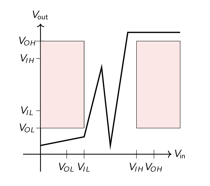
improvement 2: divide signals range into input and output area. V_OL < V_IL < V_IH < V_OH.
- an output of a 0 or 1 from some device won’t turn into an undefined or opposite bit when it is read into another input device.
Analysis: analog systems accumulate noise, while digital systems can manage to solve the problem mostly, so that the noise will be canceled at each stage in digital systems.
- Problem: buffer: copy one bit(input->output)
- Voltage transfer characteristics: Active components(gain > 1)

- Voltage transfer characteristics: Active components(gain > 1)
- digital circuits: two kinds, combinational circuits and sequential circuits.
5 CMOs
Problem: how the gates are built?
-
CMOs technology(Complementary metal-oxide semiconductor): packaged chip, silicon die, transistors as voltage-controlled switches
-
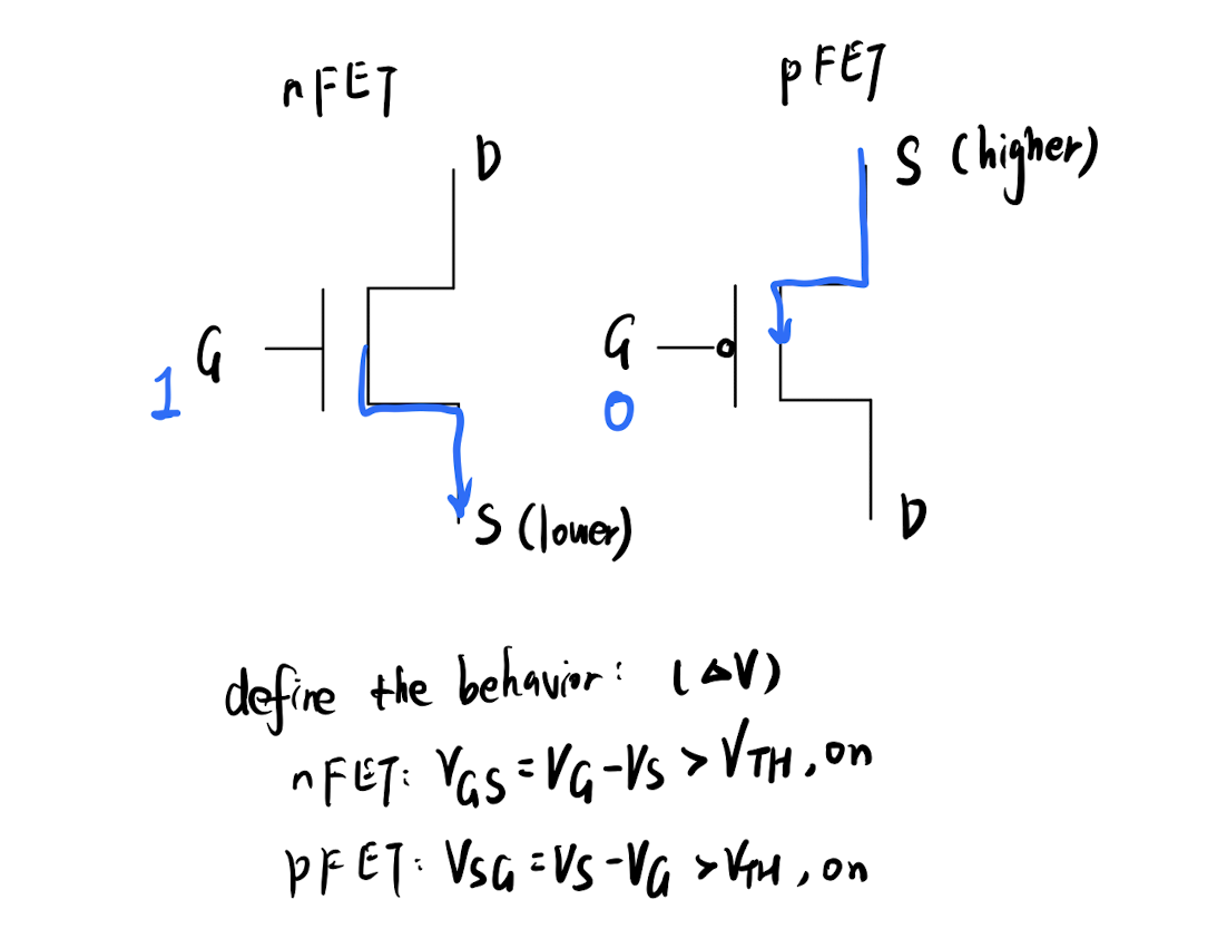
field effect transistor(FET) has three terminals: gate, source, drain.
-
Two types: nFETs, pFETs

-
Two examples to explain the behavior
- NOT gate: threshold V_TH, range(if V_IN < V_TH, on; if V_IN > V_DD - V_TH, off)
- NAND gate
-
-
functional behavior of transistors for building logic gates
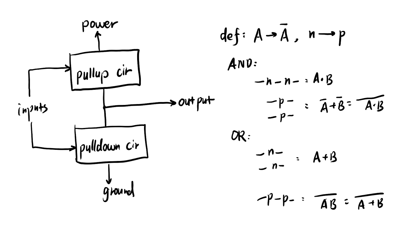
- complementary behavior: the pullup and pulldown networks are related in a complementary way, so that the pullup is on when the pulldown is off, and vice versa.
- Two problem case
- Power supply and ground are both connected to the output -> burn the circuit(driven X)
- Output is disconnected
- Convention: In CMOS, we always use pFETs to implement the pullup network and nFETs to implement the pulldown network.
- Fact: individual CMOS gates cannot implement arbitrary Boolean functions.
- reason: CMOS gates are inverting

-
physical design:p-n juctions, capacitor, gate delay…
-
power dissipation for our CMOS gates
- Dissipation comes in two parts: dynamic power, static power
- they are extremely good at having low power consumption.
6 combinational logic
introduction
-
combinational logic has two part: function spec and timing spec
- Function has two part: truth table and boolean expression.
- Fact: all combinational functions can be specified with boolean expressions.
- Timing: propagation delay
- Function has two part: truth table and boolean expression.
-
static discipline: what is a combinational device
-
problem: how fast are circuits?
- measurement: clock periods, clock frequencies
processor will change the inputs into our system and read the outputs. So we need to read the inputs correctly before it is changed later.
Problem 1: we need an upper bound to ensure that we can get the input in the worst-case.
idea: combinational contract
- Measurement: contamination delay(lower bound)
-
Boolean algebra
-
Any Boolean algebra can be derived from AND, OR, NOT
-
duality principle holds for all expressions
-
Properties: commutativity, associativity, distributivity…
1
a + (b * c) = (a + b) * (a + c) # distributivity
-
-
Truth table => boolean expressions
-
construct a normal form: sum of products
-
Simplify: minimal sum-of-products -> use algebraic manipulation(reduction, complements…)
-
to reduce the number of gates
-
Tradeoff: more gates or increase levels leading to increase propagation delay
(in this class, minispec takes care for us.)
-
remark: synthesizing optimized circuits is a very hard problem
-
-
-
boolean expressions => circuits: logic synthesis
- Term: logic gate, logic diagram
-
cell library: xor, nand, nor,xnor